CV versus Grid Spacing
Dilip is a co-op from the University of Arizona. He ran some simulations which produced unusual diode-CV curves. As with many other simulation problems, it turned out to be grid related. What was interesting about these CV curves was how continuous they were, even with very coarse grid.
July 09, 1996: Further requirements for Na extraction.
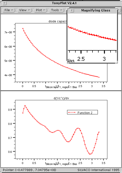
Grid spacing has been an issue for TCAD users for some time now. Process and device simulators provide an array of possibilities to users in terms of functionality, but a balance between length of simulation and accuracy should be maintained. A denser grid structure will consume more processor time, but a more accurate result can be expected due to this delay. Conversely, a coarse grid will expediate calculations, but may negatively affect accuracy. This observation may be better understood when looking at a plot of capacitance versus bias at a junction.
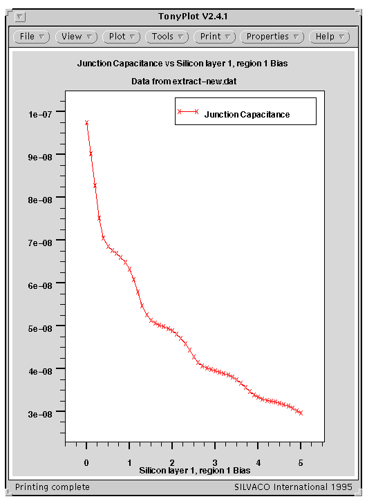
The process simulator Athena allows the user to extract electrical information from the device. By specifying an x-location in a two-dimensional structure, the simulator extracts the CV data at that point and stores the information in a file which can later be viewed. As Figure 1 uncharacteristically shows, an oscilliatory behavior is evident when 50 divisions are specified for a 2 micron region with a nominal spacing of 200 angstroms. This behavior was subsequently noticed to be caused by a relatively coarse grid.
The only assurance that the data might be correct was that the curve was negatively sloping for the NMOS device. In Figure 3, the PMOS device is shown to have a peak capacitance at a slight negative voltage, which is non-physical behavior. The grid used to produce Figures 1 and 3 had two distinct regions:
deposit silicon thick=6 c.boron=1e15 dy=0.2000
deposit silicon thick=2 c.boron=1e15 dy=0.0200 ydy=0.0200 div=50
A higher density grid seemed to be inevitable for achieving a smoother CV plot. The solution to this problem was instituting a finer grid. This time the grid had three distinct regions:
deposit silicon thick=6 c.boron=1e15 dy=0.2
deposit silicon thick=1 c.boron=1e15 dy=0.0100 spaces=10
deposit silicon thick=1 c.boron=1e15 dy=0.0100
This improved grid structure helped achieve the smooth curves seen in Figures 2 and 4.
Figure 1. Unusual oscilliatory behavior for a CV curve observed when nominal spacings of 200 angstroms are implemented with 50 divisions within a 2 micron region.
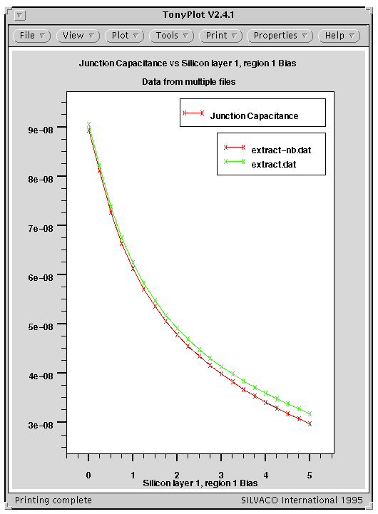
Figure 2. NMOS device comparison with an improved grid for two different processes.
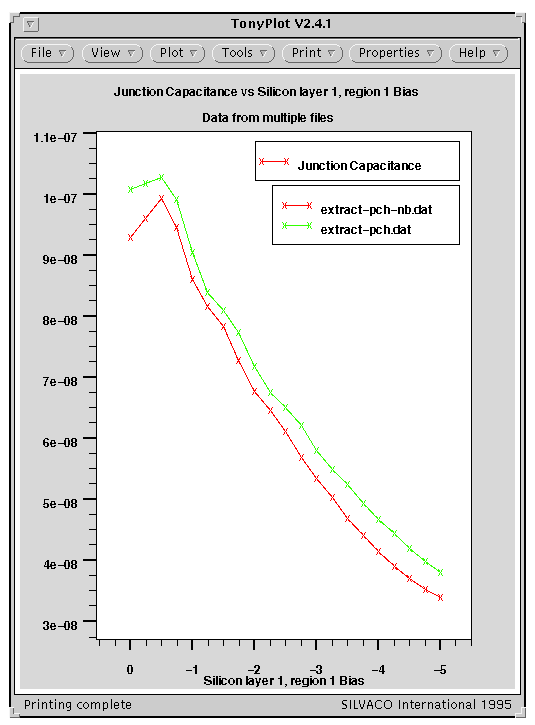
Figure 3. PMOS device comparison of a junction for two different processes.
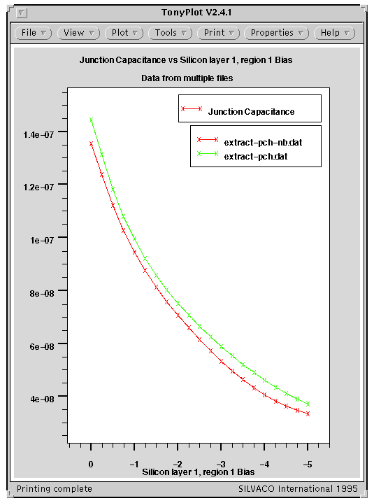
Figure 4. PMOS device comparison with an improved grid for two different processes.
Update: The derivative of 1/cap*cap with respect to voltage gives information on the dopant concentration (it's proportional to 1/N). I was running some simulations whereby the CV plot itself was rather smooth, but then d(1/c*c)/dv showed oscillations. So, having a smooth plot is not always sufficient. If you are taking derivatives, you may need even finer grid - Michael.
This page last updated November 10, 1997 by